PCB Specifications
| Features | Capability | Notes | Patterns |
|---|---|---|---|
| Layer count | 1,2,4,6 layers | The number of copper layers in the board. | |
| Controlled Impedance | 4/6 layer, default layer stack-up | ||
| Material | FR-4 | FR-4 Standard Tg 130-140/ Tg 155 | 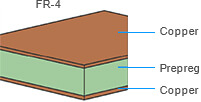 |
| Dielectric constant | 4.5(double-side PCB) |
7628 structure 4.6 2313 structure 4.05 2116 structure 4.25 |
|
| Max. Dimension | 400x500mm | The maximum dimension | 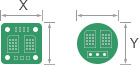 |
| Dimension Tolerance | ±0.2mm | ±0.2mm for CNC routing, and ±0.4mm for V-scoring | |
| Board Thickness | 0.4/0.6/0.8/1.0/1.2/1.6/2.0mm | The thickness of finished board. |  |
|
Thickness Tolerance ( Thickness≥1.0mm) |
± 10% | e.g. For the 1.6mm board thickness, the finished board thickness ranges from 1.44mm(T-1.6×10%) to 1.76mm(T+1.6×10%) | |
|
Thickness Tolerance ( Thickness<1.0mm) |
± 0.1mm | e.g. For the 0.8mm board thickness, the finished board thickness ranges from 0.7mm(T-0.1) to 0.9mm(T+0.1). | |
| Finished Outer Layer Copper | 1 oz/2 oz (35um/75um) | Finished copper weight of outer layer is 1oz or 2oz. | 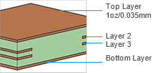 |
| Finished Inner Layer Copper | 0.5 oz (17um) | Finished copper weight of inner layer is 0.5oz only. | 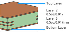 |
Drill/Hole Size
| Features | Capability | Notes | Patterns |
|---|---|---|---|
| Drill Hole Size (Mechanical) | 0.20mm - 6.30mm | Min. drill size is 0.20mm. Max drill size is 6.30mm. | 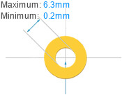 |
| Drill Hole Size Tolerance | +0.13/-0.08mm | e.g. for the 0.6mm hole size, the finished hole size between 0.52mm to 0.73mm is acceptable. |
|
| Blind/Buried Vias | Not supported | Blind vias are not supported currently, only through holes | 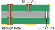 |
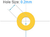
| Min. Via hole size | 0.2mm |
|
 |
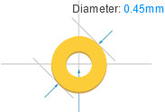
| Min. Via Diameter | 0.45mm |
|
 |
| PTH Hole Size | 0.20mm - 6.35mm | The annular ring size will be enlarged to 0.15mm in production. | 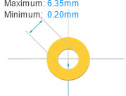 |
| Pad Size | 0.70mm - 6.35 | The pad hole size will be enlarged 0.15mm in production. | 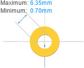 |
|
Min. Non-plated Holes |
0.50mm | The minimum NPTH dimension is 0.50mm. Please add the NPTH in the mechanical layer or keep out layer. |
 |
|
Min. Plated Slots |
0.65mm | The minimum plated slot width is 0.65mm, which is drawn with a pad. | 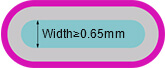 |
| Min. Non-Plated Slots | 1.0mm | The minimum Non-Plated slot Width is 1.0mm, please draw the slot outline in the mechanical layer (GML or GKO). | 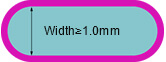 |
| Min. Castellated Holes | 0.60mm | The minimum diameter of castellated holes is 0.60mm. | 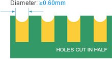 |
| Hole Size Tolerance (Plated) | +0.13mm/-0.08mm | e.g for the 1.00mm Plated hole the acceptable finished hole size is between 0.92mm to 1.13mm | 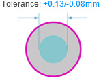 |
| Hole Size Tolerance (Non-Plated) | ±0.2mm | e.g for the 1.00mm Plated hole the acceptable finished hole size is between 0.80mm to 1.20mm | 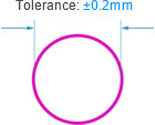 |
| Rectangle Hole/Slot | Not supported | We don't make rectangle holes/slots. The rectangle holes/slots will be made round or oval by default. |  |
Minimum Annular Ring
| Minimum annular ring | PTH | Patterns | |
|---|---|---|---|
| 1oz Copper | 0.13mm | 0.3mm | 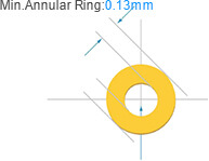
|
| 2oz Copper | 0.2mm | 0.3mm |
Minimum Clearance
| Features | Capability | Patterns |
|---|---|---|
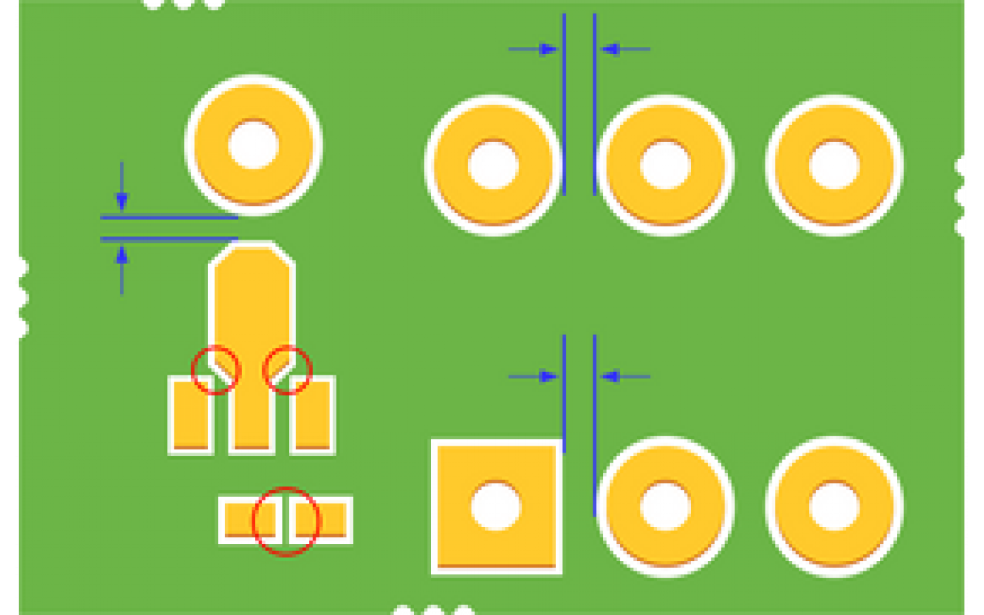
| Hole to hole clearance (Different nets) | 0.5mm | 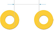 |
| Via to Via clearance (Same nets) | 0.254mm | |
| Pad to Pad clearance (Pad without hole, Different nets) | 0.127mm | 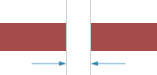 |
| Pad to Pad clearance (Pad with hole, Different nets | 0.5mm | |
| Via to Track | 0.254 |  |
| PTH to Track | 0.33mm | |
| NPTH to Track | 0.254mm | |
| Pad to Track | 0.2mm |  |
Minimum trace width and spacing
| Copper weight | Min. Trace width | Min. Spacing | Patterns |
|---|---|---|---|
| H/HOZ (Inner layer) | 5mil (0.127mm) | 5mil (0.127mm) | 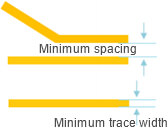 |
| 1oz (Outer layer) | 1/2 layers: 5mil (0.127mm) 4/6 layers: 3.5mil (0.09mm) |
1/2 layers: 5mil(0.127mm) 4/6 layers: 3.5mil(0.09mm) |
|
| 2oz (Outer layer) | 8mil (0.2mm) | 8mil (0.2mm) |
BGA
| Layer count | Min. BGA Pad Dimensions | Min. Distance between BGA | Patterns |
|---|---|---|---|
| 1/2 layers | 0.4 mm | 0.127mm | 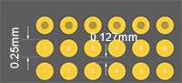 |
| 4/6 layers | 0.25mm | 0.127mm |
Solder Mask
| Features | Capability | Notes | Patterns |
|---|---|---|---|
| Solder mask opening/expansion | 0.05mm | The solder mask should have a minimum of a 0.05 mm "growth/mask opening" around the pad to allow for any mis-registration. | 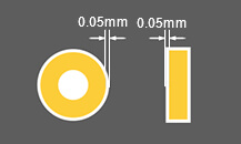 |
| Solder bridge | 0.2mm (green) 0.254mm (other colors) |
To have solder mask bridge, the spacing between copper pads edge must be 0.2mm (8mils) or more. | 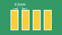 |
| Solder mask color | green, red, yellow, blue, white and black | We use LPI (Liquid Photo Imageable) solder mask. It is the most common type of mask used today. | |
| Solder mask dielectric constant | 3.8 | ||
| Solder mask thickness | 10-15UM |
Legend
| Features | Capabilities | Notes | Patterns |
|---|---|---|---|
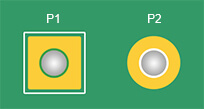
| Minimum Line Width | 6 mil (0.153mm) | Characters with width less than 6mil (0.153mm) will be unidentifiable. | 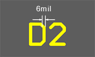 |
| Minimum Text Height | 32 mil (0.8mm) | Characters with height less than 32mil (0.8mm) will be unidentifiable. |  |
| Character width to height ration | 1:6 | The preffered ration of width to height is 1:6. |  |
| Pad To Silkscreen | 0.15 mm | The minimum distance between pad and silkscreen is 0.15mm. | 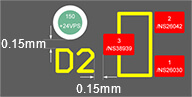 |
Board Outlines
| Features | Capability | Notes | Patterns |
|---|---|---|---|
| Trace to Outline | 0.2mm | Ships as individual board(Rounting):Trace to Outline ≥ 0.2mm | 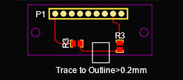 |
| Trace to V-cut line | 0.4mm | Ship as panel with V-scoring: Trace to V-cut line ≥ 0.4mm | 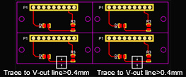 |
Panelization
| Features | Capability | Notes | Patterns |
|---|---|---|---|
| Panelization without space | 0mm | The space between boards is 0mm. | 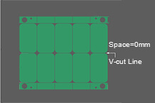 |
| Panelization with space | 2mm | Make sure the space between boards should be ≥ 2mm, otherwise it will be hard to process for rounding. | 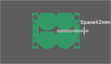 |
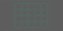
| Panelized Round board | ≥ 20mm x 20mm |
The single round board size should be ≥ 20mm x 20mm. Panelize with stamp holes and add tooling strips on four board edges. |
 |
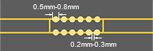
| Panelized castellated holes board | Panelize with stamp holes and add tooling strips on four board edges |
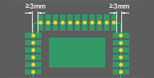
The distance between castellated hole and board corner should be larger than 4mm. Recommended diameter of stamp hole is 0.5mm - 0.8mm. Recommended distance between the two stamp holes is 0.2 - 0.3mm. |
|
| Min. Width of Breakaway Tab | 4mm | The minimum width of breakaway tab is 4mm. For breakaway with mouse-bites, the minimum width is 5mm. | 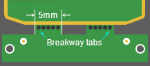 |
| Min. Edge Rails | 4mm | If choosing panel by PCBNOW, we will add 5mm edge rails on both sides by default. | 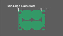 |
Csak RS-274x formátumú gerber fájlokat tudunk elfogadni a gyártáshoz!
Különböző rajzprogramok projekt fájljait nem tudjuk feldolgozni, és nem is tudunk belőle gerber állományokat készíteni ezt mindenki saját maga kell hogy elkészítse.
Mindenki ellenőrizze le hogy a saját tervező programja képes-e ilyen fájlok generálására.
A gerber állományokat tömörített ZIP fáljként kell feltölteni.
A fájlok elkészítése előtt mindenki ellenőriztesse le a saját rajz programjával hogy a gyártási feltételeknek megfelel az elkészült terv.